|
|
|||||||||
1 MEG MEMORY UPGRADE XL INSTALLATION |
CAUTION: This product should only be installed by persons with proper
training in the art of soldering. Newell Industries will not be held
responsible for damage to the computer due to neglect or carelessness. Read these
instructions completely before beginning.
The 1 MEG upgrade can be installed using different combinations of bits of
the $D301 address port of the 6520 PIA. The 130XE uses bit 4 (low) to enable Main
cpu banking, and bit 5 to enable Antic (screen pro.) It uses bits 2 & 3 to determine
which of the four 16K banks is a live. The 130 XE uses 2 sets of ram banks and flip
flops the CAS line to activate the banked memory. We use the same method to bank
into the 1 meg of ram. See below. After installation, your XL will be functionally
compatible with the upgraded XE.
$D301 PIA PORT B BIT ASSIGNMENTS (UNMODIFIED 130XE)
BIT 0-O.S. ROM CONTROL, 1=ROM, 0=RAM
BIT 1-BASIC ROM CONTROL 1=RAM, 0=ROM/NO CONNECT ON 1200XL
BIT 2-RAM BANK SELECT, 1=RAM, 0=RAM/NO CONNECT ON XL
BIT 3-RAM BANK SELECT, 1=RAM, 0=RAM/NO CONNECT ON XL
BIT 4-CPU BANK ENABLE, 1=NOT ENABLED, 0=ENABLED/NO CONNECT ON XL
BIT 5-ANTIC BANK ENABLE, 1=NOT ENABLED, 0=ENABLED/NO CONNECT ON XL
BIT 6-NOT USED
BIT 7-DIA.ROM CONTROL, 1=RAM, 0=ROM
GENERAL INSTALLATION
The ribbon cable H2 wires (RED)1=HALT, 2=DEL, 3=REF, 4=ABO, 5=AB1, 6=AB2,
7=AB3, 8=AB4, 9=AB5, 10=AB6, ll=CASO, 12=CASI, 13-14=SPARE.
The ribbon cable H3 wires (RED)1=Al4, 2=Al5, 3=A6, 4=A7, 5=SPARE, 6=S,
7-14=D7-D0.
l. Disassemable computer and remove the motherboard. Install eight l meg ram chips
on the 1 meg board, Ul-U8, notch towards the caps.
1200XL ONLY
A. Cut trace to pin 3 of U7. Cut trace to pin 11 of U10. Cut trace to pin 13 of
U10.
NOTE:Make these changes on the bottom of the mother board.
B. Install jumper wire from CPU address A7 to U10 pin 11. A7 is the trace that
was going to U7 pin 3.
C. Install jumper wire from CPU address A13 to U7 pin 3. A13 is the trace that
was going to U10 pin 13.
D. Install jumper wire from CPU address A14 to U10 pin 13. A14 is the trace that
was going to U10 pin 11.
E. Test computer before proceeding.
2. Remove the ram chip from U13(8OOXL), U6(1200XL). Install Hl cable in U13 or
U6. Make sure that pin 1 matches up. Solder or socket. Install the 64K ram chip
in U17. Fold the cable and place the 1 meg board on top of the motherboard
component side up.
3. Connect DO-D7 data lines to pins 30-33 and 40-37 of the Antic rom. Cut these wires
so there is not a lot of excess slack in the wires. But don't make them tight.
4. Connect REF to pin 8 of Antic. Connect HALT to pin 9 of Antic. Connect DEL to
pin 9 of U30(800XL), U25(1200XL).
5. Remove pin 8(CAS) of U30(800XL), U25(1200XL). Connect CASO where you removed
the pin. Connect CASI to pin 8.
6. Connect A6 to Antic pin 26, connect A7 to pin 25, connect A14 to pin 19,
connect A15 to pin 20. Connect S to pin 10 of U29(800 XL), U22(1200XL).
7. Install the control lines per preferred method listed, or any other way you
like.
8. Make sure that the l meg board is not shorting to anything and turn the
computer on. If installation was done properly the computer should come up in
the same manner that it did before this installation was done. If not, correct
the problem (see trouble shooting) and try again.
9. When putting the computer back together, use extreme caution to make sure
that the l meg board does not short out anything. You may not be able to install
the top RF sheild. Don't force it.
Installation of control lines and board configuration
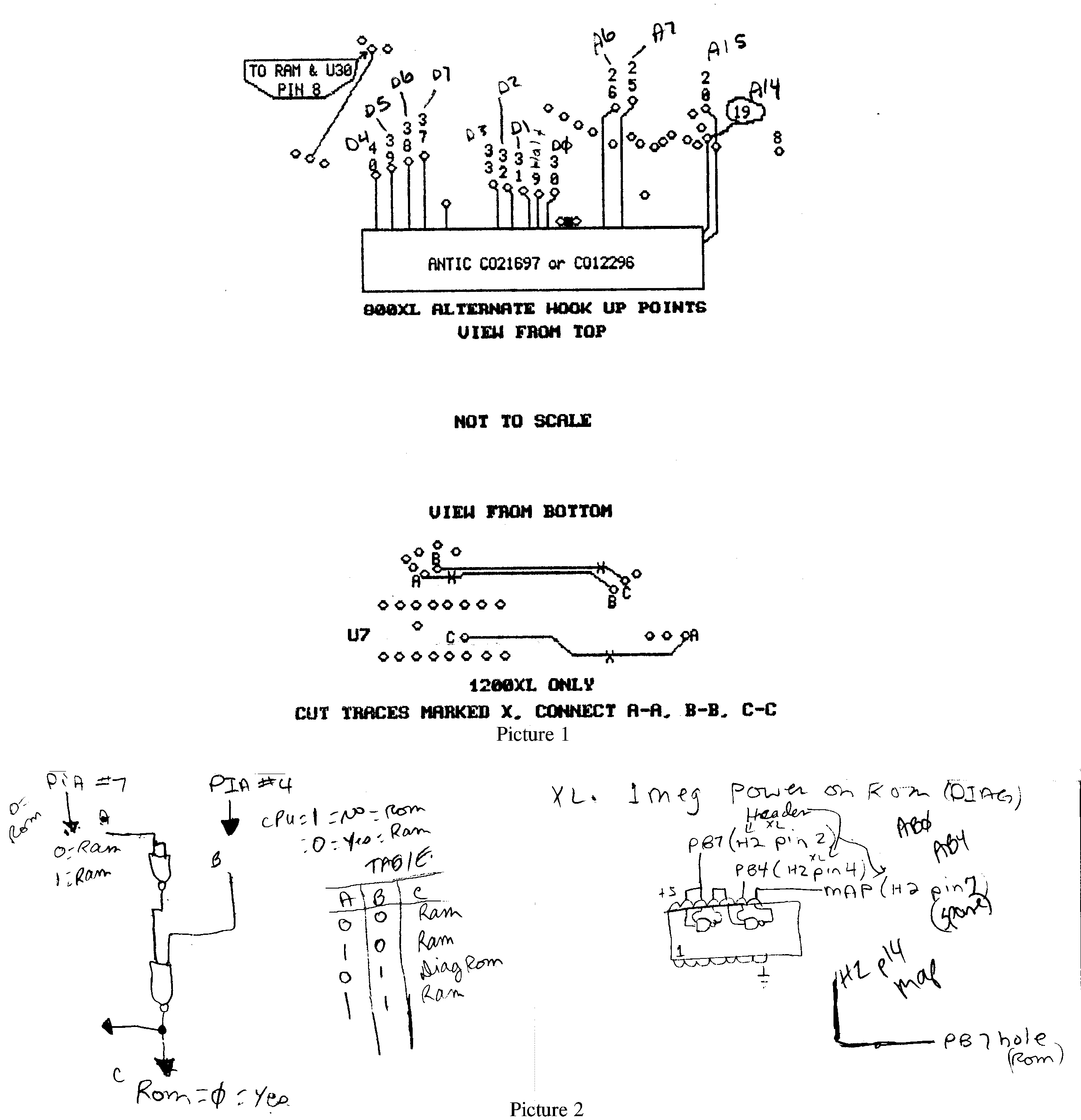
Please refer to picture 1 for motherboard details.(RLD)
Method 1
This method is comparable with Basic XE, the translator disk, and any
other software that requires bit 0 to remain in its normal configuration. This
method does allow Antic control via bit 5. With this method, internal basic is
lost via software control. This is probably the most compatible method, and the
one that I use and reccomend.
$D301 PIA PORT B BIT ASSIGNMENTS (METHOD 1)
BIT 0-O.S. ROM COMTROL, 1=ROM, 0=RAM(NOT BANK RAM)
BIT 1-RAM BANK SELECT, 1=RAM, 0=RAM(SEE NOTE BELOW)
BIT 2-RAM BANK SELECT, 1=RAM, 0=RAM
BIT 3-RAM BANK SELECT, 1=RAM, 0=RAM
BIT 4-CPU BANK ENABLE, 1=NOT ENABLED, 0=ENABLED
BIT 5-ANTIC BANK ENABLE, 1=DISABLED, 0=ENABLED/RAM BANK SELECT, 1=RAM, 0=RAM
BIT 6-RAM BANK SELECT, 1=RAM, 0=RAM
BIT 7-RAM BANK SELECT, 1=RAM, 0=RAM (SEE BELOW)
l. On the PIA, remove pins PB1(11), and PB7(17) from the motherboard and bend
them out. Be careful not to damage the motherboard or break the pins off at the
IC.
2. Connect a toggle, or momentary switch between PB7 pin 17 and motherboard
where PB7 was connected. Not required on standard,1200XL.
NOTE:This switch must be closed during power up (Atari and Omniview OS's) until
you get a screen. It can be left off in OSNXL. If you want to use the internal
diagnostics, or you go into omnimon of OSNXL, then the switch must be on(closed).
It must also be on while you go into 80 columns of Omniview. Turn it off(open)
all other times).
3. Connect wires ABO to PIA PB7(pin 17), AB1 to PBl(11), AB2 to PB2(12), AB3 to
PB3(13), AB4 to PB4(14), AB6 to B5(15), AB6 to PB6(16).
4. To be able to select the internal basic, (800XL), connect a toggle switch
between ground and the motherboard where PB1 was removed. The switch is not
much different than the Option Key, and I found it more versatile.
5. Jumper Jl on 1 meg board.
Method 2
This method is compatable with Basic XE, the translator disk, and any
other software that requires bits 0 and 1 to remain in their normal
configuration. This method does not allow Antic control. If Antic addresses the
banked memory area ($4000-$7FFF), it will see the banked memory currently
there. Okay, here's what we do. We are going to to connect the lines that
normally go to the enable bits to ground. This will mean that the 1 meg banked
memory area is always active so we are going lose the 16K bank of main memory,
and replace it with 16K of the banked memory. This will cost you 16K of ramdisk
for a total of 1008K available.
$D301 PIA PORT B BIT ASSIGNMENTS (METHOD 2)
BIT 0-OS ROM CONTROL, 1=ROM, 0=RAM
BIT 1-BASIC ROM CONTROL, 1=RAM, 0=ROM
BIT 2-RAM BANK SELECT, 1=RAM, 0=RAM
BIT 3-RAM BANK SELECT, 1=RAM 0=RAM
BIT 4-RAM BANK SELECT, 1=RAM, 0=RAM
BIT 5-RAM BANK SELECT 1=RAM, 0=RAM
BIT 6-RAM BANK SELECT, 1=RAM, 0=RAM
BIT 7-RAM BANK SELECT, 1=RAM, 0=RAM (SEE BELOW)
l. On the PIA, remove PB7 from the motherboard and bend it out. Be careful not
to damage the motherboard or break the pin off.
2. Connect a toggle, or momentary switch between PB7 pin and board.
NOTE:See note in method 1.
3. Connect wires ABO to PB7, AB1 to PB4, AB2 to PB2, AB3 to PB3, AB4 to Ground,
AB5 to PB5, AB6 to PB6.
4. On the 1 meg board, jumper JI OPEN (no jumper).
Method 3
This method is NOT compatable with Basic XE, the translator disk or any
other software that requires bits 0 and/or 1 to remain in its norma
configuration. This method does allow Antic control via bit 5. With this
method, internal basic is lost via software control. Access to the ram under
the OS is also lost.
$D301 PIA PORT B BIT ASSIGNMENTS (METHOD 3)
BIT 0-RAM BANK SELECT, 1=RAM, 0=RAM
BIT 1-RAM BANK SELECT, 1=RAM, 0=RAM (SEE BELOW)
BIT 2-RAM BANK SELECT, 1=RAM, 0=RAM
BIT 3-RAM BANK SELECT, 1=RAM, 0=RAM
BIT 4-CPU BANK ENABLE, 1=NOT ENABLED, 0=ENABLED
BIT 5-ANTIC BANK ENABLE, 1=DISABLED, 0=ENABLED / RAM BANK SELECT, 1=RAM, 0=RAM
BIT 6-RAM BANK SELECT, 1=RAM, 0=RAM
BIT 7-DIA. ROM CONTROL, 1=RAM, 0=ROM
1. On the PIA, remove pins PB0, and PB1 from the motherboard and bend them out.
Be careful not to damage the motherboard or 'break the pins off.
2. Connect wires AB0 to PB0, AB1 to PB1, AB2 to PB2, AB3 to PB3, AB4 to PB4, AB5
to PB5, AB6 to PB6.
3. To be able to select the internal basic (800XL), connect a toggle switch
between ground and the motherboard where PB1 was removed.
Helpful hints:
If you have read these instructions and do not understand them, then do
not attempt this installation without assistance.
TROUBLE SHOOTING
1. BLANK SCREEN
This could be caused by numerous things. Did you close the PB7 switch?
Check all ICs for bent pins. Check for shorts in soldering. To isolate problem,
remove the 1 meg board. If you have used method 2 remove the grounds for bank
enabling and power up again. If problem is in l meg board, system should come up
normally.
2. MYDOS WILL NOT BOOT-ERROR MESSAGES DURING TEST RUN
Check solder connections for bad solder joints or shorts. Check ABO-AB6 to
proper pins.
3. UNKNOWN
The chances of your having a defective 1 meg board are very small. THE
MOST COMMON CAUSE FOR PROBLEMS ARE IMPROPER INSTALLATION. If you have double
checked your installation and it still does not work, contact the newsgroup
comp.sys.atari.8bit(2002).
USING YOUR 1 MEG RAM
There is a simple program that checks one byte of each bank of memory to
insure that they are working. It is on the disk furnished. The filename is
"MxTESTlM.BAS" (X reffering to installation method 1, 2, or 3). When this
program is run, it should come back with "TEST COMPLETE, 0 ERRORS". If you get
any ERROR messages back, refer to the trouble shooting section. CAUTION, reboot
your system after running this program. It alters memory, and may have some
undesirable affects if the system is not rebooted.
MYDOS DISK OPERATING SYSTEM
The MYDOS disk operating system 4.50.Ml furnished with the l meg upgrade is
a patched version of 4.50. The patch was made to correct a problem in the
ramdisk handler that would not allow the use of bits 0 and 1. Refer to the
Mydos manual for setting up the various types of ramdisks available. The page
sequence table in Mydos starts at $0BBA and is high nibble C,A,8,6,4,2,0,E by
low nible 1,3,5,7,9,B,D,F as shipped with this upgrade configured for method 1
installation.
M1COPY SECTOR COPIER
This program was designed to be used with the method 1 installation of the
1 Meg upgrade. It should not be used with any other computer unless it is
verified that it uses the same bank switching methods. The program resides at
$8500, once loaded may be rerun usin the M option of DOS to run at $8500
(assuming it has not be overwritten by another program).
The ramdisk page sequence of the MYDOS with the upgrade is such that the
copy program may be ran and copy as many disk as you like and return to DOS
without loosing the RD directory including DUP.SYS and MEM.SAV. The ramdisk
will not even know that part of it was used. Of course, if the ramdisk is full,
you will loose the files in the last portion depending on the size of disk you
copy. The page sequence for M1COPY is high nibble 0,2,4,6,8,A,C,E by low nibble
1,3,5,7,9,B,D,F. COpying a 720K disk will only go up to the A7 bank thus
leaving the normal 130XE banks and the dos lower ramdisk banks alone.
Use the 'L' command from DOS to load M1COPY. If you are going to copy 80
track or double sided diskettes, your disk drives must be configured prior to
running the program. The program can be loaded from the ramdisk if you need to
configure ygur drives. M1copy uses ONLY the banked memory area for copying, so
nothing special is required.
The first prompt. HOW MANY COPIES?
Enter how many copies you want (1-99) and, if needed, the special
characters to pass information to the program.
SPECIAL CHARACTERS
A "D" entered after the number of copies (exp. 25D) indicates that the
diskette you are going to copy is a double density diskette.
A "Q" indicates that you want to copy 1440 sectors per diskette (exp.
25DQ). This could be a 40 track double sided, 80 track single sided, or 80 track
double sided diskette that you only want to copy the first 1440 sectors.
Remember that the format option will format the new diskette to the
configuration of the drive.
An "O" indicates that the diskette you are going to copy has 2880 sectors.
(exp. 25DO) This would be an 80 track double sided diskette.
An "H" indicates that you just want to copy the first portion of the
diskette, including the directory (369 sectors) (exp. 25H). This example would
copy the first 369 sectors of any single density diskette.
NOTE: The last character entered will be the one used by the program (exp.
IDHQ translates to 1DQ, 99QOHD translates to99HD) A "Return" without a
specified number of copies will be interpreted as 153 (exp. H translates to
153H) "Return" must be after entry. (exp. lH"Return").
SOURCE DRIVE?
Enter the drive number where you will put the diskette to be copied (1-4).
Do not press "Return". Drive density is automatically set on source aisk.
DESTINATION DRIVE?
Enter the drive number that you will use to write the copies to (1-4). Do
not press "Return". Drive density must match source diskette. Using the same
drive for source and destination will insure that the density matches.
VERIFY WRITES (Y OR N)
Press "Y" if you want to write with verify. This takes about 3 times
longer to copy a diskette and is normally not used unless you have some very
important diskettes to back up.
FORMAT (Y or N)?
Press "Y" if you want the destination diskette formatted automatically
with every copy. Otherwise press "N". Do not press "Return".
INSERT SOURCE DISK, PUSH START
Follow this prompt to read your source diskette.
INSERT DESTINATION DISK, PUSH START
Follow this prompt to write your copies.
UNREADABLE SECTORS
If unreadable sectors are encountered, after a few tries, the program will
continue to the next sector using whatever data it got from the bad sector to
write to the destination disk, until the end sector is reached. This program is
not intended to copy copy protected diskettes. Be aware that it is illegal to
copy copyrighted software for any purpose other than backup.
1 MEG UPGRADE MODS
1. ELIMINATE POWER UP SWITCH ON 1 MEG 8 BIT UPGRADES
1 MEG 130XE:
Install a 74LS00 chip in the spare socket. Place the chip in the bottom portion
of the 16 pins. Strap socket pin 16 to 15 (power to LS00 pin l4).
1 MEG XL:
Bend up all pins except 7 & 14 on a 74LS00. Piggyback the 74LS00 on top of the
74LS393 in U11 and solder pins 7 & 14 (ground & +5V).
ALL:
On the 74LS00 strap pins 12 to 13 to PB7 (H2 pin 2 on XL, H2 pin 15 on XE).
On the 74LS00 strap pin 11 to 10.
On the 74LS00 strap pin 9 to PB4 (H2 pin 4 on XL, H2 pin 13 on XE).
On XE only, connect wire 15 to PB4 (PIA pin 14).
Remove the power up switch between PB7 pin and PB7 hole (PIA pin 17).
On the XL, make sure the 74LS00 pins do not short out on the RF sheild or
opposing components.
Test computer.
THEORY OF OPERATION:
PB7 is inverted thru pins 12 & 13 to pin 11 which is connected to the input of
the controlling gate at pin 10. PB4 is the second input to this gate at pin 9.
The output at pin 8 (MAP) is low (ROM) if both inputs are high, otherwise the
ouput is high (RAM). This allows normal operation until banking occurs
(PB4=low). At this time the MAP goes high, forcing the computer to map to
ram.
NOTES:
The only problem that could be encountered, is if software was doing memory
banking and tried to bank in the rom. I can think of no software that would do
this since the rom at $5000-$57FF would overshadow the ram in these locations
thus voiding the ram. Omnimon in the OSNXL OS does bank in the rom to execute
some of its commands, but functions normally as long as you don't force
banking.
I have included a picture(#2) on the wiring of the 74LS00 I used.(RLD)
(rev 2, 24aug02)
|
Want more info on ram? ars-technica
RLD
