|
|
|||||||||
This file is o.k. for printing, but you can DL SIMM UPGRADE.ZIP for this webpage with high res pics. Pounding on the 8 Bits Buy your own/share what you know/8 bits are plenty |
|
April, 1992 by Bob Woolley This month's article is written for those guys over at OL'HACKERS. Hope they like it! How about we talk about RAM upgrades? There are quite a few of them out there to choose from - maybe this will help sort them out a little. A RAM upgrade adds more memory to your computer. Simple. What isn't so simple is how you access that memory. It would be so nice if it worked like the old 800s, you add the memory and the operating system starts using it. Basic, DOS, everybody gets to use more RAM (Random Access Memory). Problem with these new upgrades (past 64K) is that the OS, ANTIC, and the 6502 CPU can't use any more than 64K at any one time. Once they count up to 65535, they must wrap back down to 0 and start over since there are only 16 address bits. Think of it as spaces in a parking lot where you can number them using only two digits - you will only get 100 numbered spaces, 0 to 99. As a consequence, memory upgrades must bank in the new memory over existing data, swapping the two data spaces with each other. What used to be your Basic program, for example, will now be disk sectors while the memory is swapped. This is called banking and is the technique used in all these hacks. When you design such an upgrade, you must first consider where in memory and how much you will bank select for the extra memory. Banking out 256 bytes (1 page) of memory would require a lot of switching and swapping to be useful with a large data field such as the text buffer of a word processor, for example (it would be fine for a ramdisk, though - maybe some time in the future we can try that approach). Banking all 64K would crash the system since your program would also be banked out, no matter where it was in memory. The 13OXE uses a 16K bank, 25% of your available memory space. Since the OS ROM sits in the last bank and the first bank has OS variables and the stack, the only choices were the second and third banks. The third bank will often have a cartridge active in it, so we really only have one choice - bank two, from $4000 to $7FFF. The bank that is active is controlled by the register in location $D301, which is also used as a control for certain ROM, cartridge and RAM access on XL/XE machines. To use an extended bank of data, you must first be sure that no interrupt routines will be called in $4000 thru $7FFF. If any interrupt vectors into your banked memory, it will probably try to execute a sector of ramdisk or something equally destructive. For the most part, this is not a problem - few programs seem to use this bank in such a manner. The routines in your program that will control the bank will also have to be located outside the bank area unless you have made some special arrangements to duplicate them in the target banks. Banking is done by setting bit 4 low at address $D301. Once bit 4 is low, any access to $4000-$7FFF will see RAM selected by the bank address bits, usually bits 2,,3, 5, and 6 at $D301. In the case of a 13OXE, setting bit 4 low actually enables the second row of RAM chips, and all banks are extended memory (using bits 2 and 3, you get 4 16K banks of extended memory). Most XL upgrades use only one set of RAM chips which results in some of the extended banks actually being the normal RAM space. For example, using bits 2, 3, 5, and 6 on a RAMBO upgrade will give you main RAM banks in $4000-$7FFF whenever you set bits 5 and 6 low (since you have 16 16K banks and only 256K of memory, all banks are selectable). What we are considering here is a very large memory space, 1 meg and larger. Our available bits in $D301 are really only 2, 3, and 6, but common practice also uses bit 5. We can also use bit 7 by using some control logic and bit 1 if we give up internal Basic. Any other bits used (0 or 4) will cause gross compatability problems with the OS and other software. So, unless we use a separate register somewhere, we can only select 64 16K banks, four of which are going to be our main memory banks. This will still allow 960K of expanded memory - not too bad! There are essentially two types of upgrades, ANTIC compatible and non ANTIC. Newell, 130XEs, and my own upgrades are ANTIC banking. ICD (RAMBO), and many other individuals upgrades do not bank. An ANTIC compatible upgrade makes allowance for separate access to the extra RAM between the CPU or the ANTIC screen processor. You must realize that two different subsystems in your Atari 8-bit use memory - ANTIC and the CPU. Normally, the 6502 CPU is getting instructions and data from your memory chips and executing the program that you have loaded. However, the ANTIC screen processor chip is also executing a program (called the display list) and whenever it needs data or instructions from your RAM chips, it just stops the 6502 and takes what he needs from memory. If you are using some form of memory upgrade, the data in memory between $4000 and $7FFF may be banked out when ANTIC comes looking for it's data. This is going to cause quite a mess unless you design the circuitry to allow for it. The 13OXE solution to this problem is to have the control register bit 4 control CPU banking and bit 5 control ANTIC banking. The down side of this method is the extra circuitry required and the loss of potential bank(s) addressing bits in $D301, the control register. It is quite unfortunate that the most widely used memory upgrade, RAMBO, did not choose to follow the ANTIC banking and used bit 5 as a bank selection bit. As a consequence, the majority of commercial software that uses extra memory follows the RAMBO standard. Those upgrades that follow the proper use of bit 4 and 5 will therefore not work properly on commercial software. This is just added incentive to use bit 5 in any design. One more factor - chip selection. The Atari computers use 16 pin, 64K memory chips. The 256K chips that are used to upgrade memory are also 16 pin - making it easy to go to 256K. I wish the 1 meg chips were 16 pin, then that would be a cinch also. But they aren't. They are 18 pin devices. You can't just pop them into our old 64K locations. Some upgrades solder additional 256K chips on top of the existing ones. This is not a good idea. Each RAM chip (there are 8 memory chips) draws about 50ma. of current. Total:400ma. This is about one third of the current used by the whole computer. Adding one set of RAM chips will increase your current drain by maybe 33% - not real bad, but significant. Adding three more sets of RAM chips (to get to 1 meg) is foolish. You just have to use 1 meg chips (which only draw about 50ma. each). If you want to go to 4 meg, you must use 4 meg chips for the same reason. This means a whole new board for the RAM as well as the control circuitry. The Newell is done this way and the one I did is done this way. Newell uses (dram)chips, I used SIMMs - same difference. One more thing - refresh. The RAM chips work like microscopic batteries, you charge them up to store a "1" and discharge them to make a "0". The fact that you have to be able to do this very quickly, makes this a very weak battery - it goes "dead" in less than a second. What is then required is to read the data in each battery and restore the cell to full charge if it is supposed to be a "1". This is called "refresh" and is performed about 60 times per second on each cell. The Atari has the bits to do this built into the ANTIC chip, who, along with its other duties, sends out a refresh signal every so often. Biggest problem for us is that ANTIC was designed to refresh only 64K on a 1200XL and 256K on an 800XL or 130XE. It will never send refresh to the memory above 256K - making it useless. Not having much use for useless memory, I looked closely at the 1 meg chip parameters. Seems that 1 meg chips will refresh themselves if you tell them to, all 1 meg. What is needed is just an AND gate that combines the -REFRESH and -CAS lines of your Atari (ref. figure A). Even the old 64K ANTIC in a 12OOXL will then work with 1 meg or 4 meg chips - the address counters are in the RAM chips themselves! So, enough background, let's build an upgrade. The extended RAM is selected whenever A14 is high, A15 is low, and PB4 is low on the 6520 ($D301). The select bit enables two selector chips (74HC157s), one to bank address and the other to gate PB7 and MA7. The bank address is staightforward, portb bits are selected thru the '157 by the same clock used on the main board to multiplex the other address bits. The MA7 source is from pin 9 of the U10 when in normal mode, and from the '157 multiplexer when banking. The PB7 selector (which controls the diagnostic portion of the OS ROM) allows bank selection whenever we are banking and diagnostic selection when we are not. This works well since diapostics are only called during bootup, when you are always in normal mode. Construction was done on a perf board with a bunch of wires down to the main board. This is a little messy, but not too bad. Many of the SIMM lines, by the way, can be interchanged. As long as the data and a come out the way they go in, who cares what the chip thinks they are (by that I mean A6 can be swapped with A1 and like that. You can't swap data with address, of course). I'd much prefer a plug-in approach, but there just isn't anyplace that contains all the required lines. The locations called out are for a 1200XL. There are similar points in the 800XL which should produce identical results. Not that much to it - four chips and a simm for 1 meg. Next month, we may add some more controls and do 4 meg. This will probably use a different control register and switch in four 1 meg ramdrives, since MYDOS can only access a maximum of 1 meg in it's rammdisk handler. I tried the upgrade using the Newell 1 meg MYDOS version and it seems to work OK. The machine itself has been running well (I did most of this article on it with no strange crashes or loops. SpartaDOS cartridge does not function, I'm afraid. SpartaDOS itself only sees a 32OXE, as do most commercial programs.... I'll tell you something - loading 1 meg takes a long, long time from a disk drive. Once I get it loaded, I hate to power down. See you next month! Note: The NEWELL 1 meg MYDOS must have the selection sequence modified such that the last three bytes in the table are $07, 05, 03, 01. I set my table to read(all hex, starting at $BBA): EF, ED, FB, E9, E7, E5, E3, El, CF, CD, CB, C9, C7, C5, C3, C1, AF... 8F... 6F... 4F... 2F... 0F... Make sure to use MYDOS 4.5.1M or newer, as it will have a 1 meg patch.(RLD) Use the 'O' command from the DUP.SYS menu and select an XE compatible, 960K ramdisk. Then alter the table at $BBA (I used the EDASM cart). Write this new DOS to a disk. This will give you the proper 960K ramdisk. REW 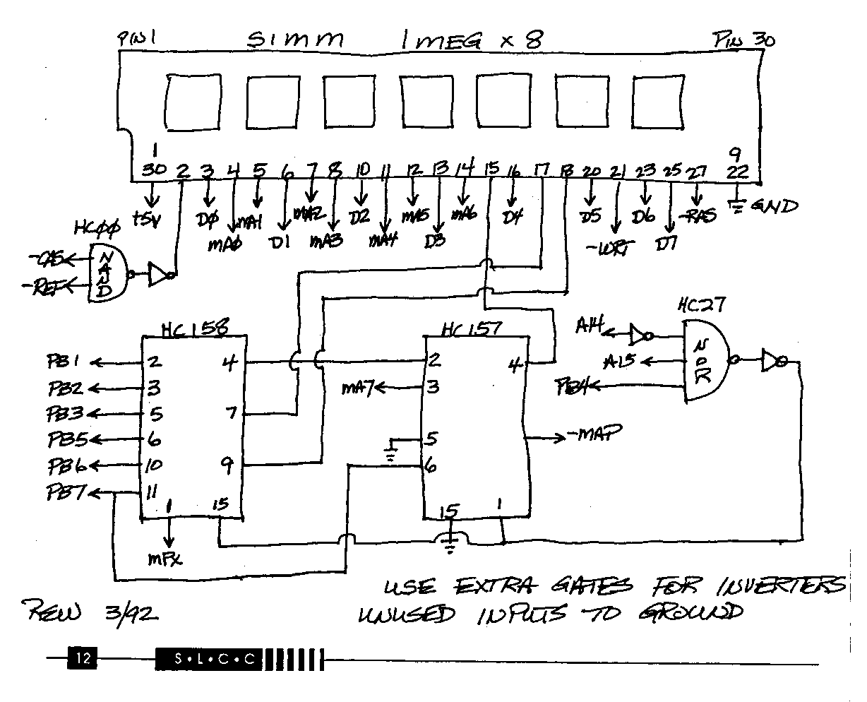
Pin connections to board: |
END
| |
|
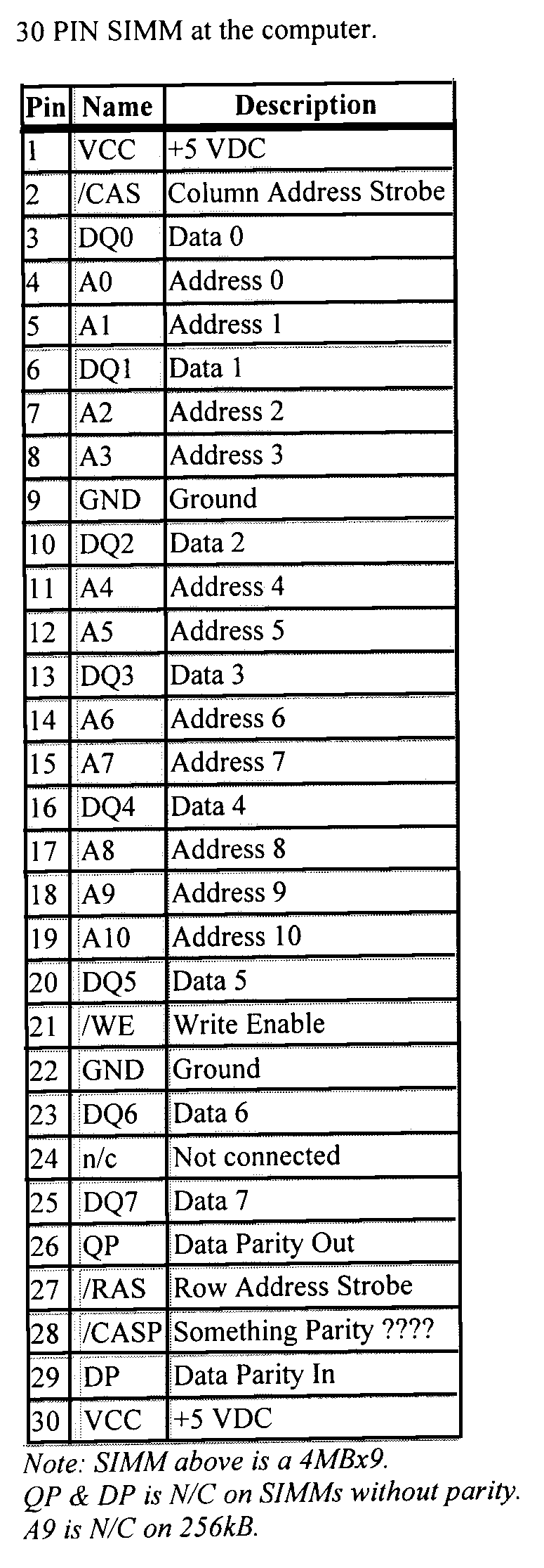
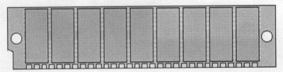
| The following page is a re-do of a 30 pin SIMM connector page I got from "www.fbe.fh-frankfurt.de/mitarb/schellha/ic/hwb/co_Simm30.html". But this Connector Site is gone(01Oct01). 30 pin SIMM SIMM=Single Inline Memory Module | |
|
 (1)---------At the Computer----------(30) |
Want more info on ram? ars-technica
RLD
